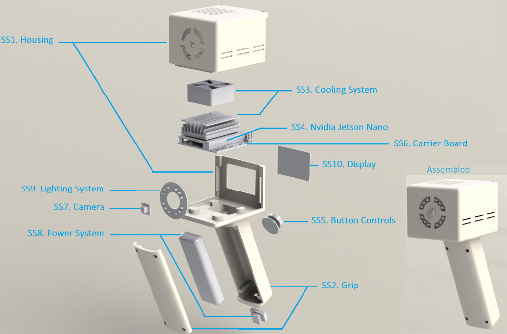
This semester, I am part of a team responsible for designing a NVIDIA sponsored medical device for use in pediatric care. The project is deep learning oriented, and I am eager to be part of the process.
The main functions of this device are to take a photo of a pediatric skin lesion using two types of light and pass the images through a convolutional neural network. A diagnosis and percentage of accuracy of that diagnosis are then displayed on the screen. This device is unique when compared to similar applications utilizing cell phones due to the fact that the processing is done locally with the Jetson Nano microcontroller provided by NVIDIA.
Below are a few writing samples and diagrams submitted for the project.
Preliminary Environmental Impact Assessment
Environmental preservation requires an accountability system.
Manufacturing Related Environmental Impact
Shell Manufacture: For the device casing manufacturing, the environmental impact created by additive manufacturing processes is significantly less than that of other conventional processes that require material removal. Since the device will be 3-D printed and not machined from solid blocks of plastic, the waste created by material removal is non-existent. However, materials considered, such as ABS, are petroleum-based polymers which give off fumes when melting and hardening. These fumes can cause eye, skin, and respiratory tract irritation. If one is overexposed to the manufacturing process, it could cause nausea and headache [5 Reasons]. The device created by the team will be a “one-off” and will not be mass-produced. Manufacturing will also take place at a well-ventilated machine shop, so pollution impact is expected to be infinitesimal. Another economic impact to consider is energy usage by the 3-D printer. According to [Compare Formlabs], the Formlabs Form 2 printer, which is the expected printer the team will use to manufacture the shell, requires 220 watts. This is approximately a fourth of what a microwave uses. Even though the printer will run in excess of 10 hours in printing the shell, its total power usage will only amount to 2.2 kilowatt-hours. For perspective, the average U.S household uses 30 kilowatt hours per day [Frequently Asked Questions].
Printed Circuit Board Manufacture: PCB board production is continuously transferred to China for three reasons: less stringent environmental policies, competitive price advantages, and China becoming the largest consumer electronics market in the world (2). Copper and ammonia are the main pollutants in wastewater resulting from designing and producing PCB boards (2). Moreover, copper waste is created during the etching process where undesired foil is etched away with chemicals such as NH4OH and NH4Cl (9). These etching solution components are the main source of ammonia. Other materials including acid, metals, etching chemicals, and various other solutions used in the process make wastewater treatment difficult and complex (9). Air, water, acoustic, oil, and greenhouse gas pollution illustrate the environmental impact of shipping. Air freight is the most efficient method of transportation, yet despite being low in air pollutants, sea shipments account for more annual tonnage. Due to great distances, increase in the amount of shipping, and substantial tax privileges, sea shipping contributes significantly to global emissions (6).
Author(s): Gabriel J. Ragusa, Christine B. Wiley
Operation/Usage Related Environmental Impact
The device operates entirely off of electrical power and produces no emissions. While deployed, the device operates off of a rechargeable battery, and when docked it is charged through a wall outlet. When operating at high power mode, the Jetson Nano consumes up to 10 W of power [Jetson nano datasheet]. A rough estimate for the time it will be operated for during each diagnosis is approximately 10 minutes given initial startup, image capture, diagnosis, and transfer to medical records. If it is assumed that it operates at maximum power consumption for the entire duration of use, then the approximate energy usage for each diagnosis is approximately 1.67 Watt-hours.
End-Of-Life (Disposal) Related Environmental Impact
Shell Disposal: For the shell, a highly considered material for manufacture is ABS. ABS is a petroleum-based, non-biodegradable plastic [5 Reasons]. Therefore, the material will not decompose if dumped into a landfill. It can, however, be recycled so that the material is not wasted, but is repurposed. It is therefore recommended that the device shell be placed into a plastic-accepting recycling bin once its end of life is reached. The energy required to recycle the shell is unknown, as different recycling processes have different energy requirements. Energy usage will be relatively infinitesimal, however, as it will be only a parcel in the millions of pounds of material recycled every day.
PCB Disposal and Recycling: PCBs have long life spans but can become defective. They contain non-biodegradable and sometimes hazardous waste materials. Non-biodegradable materials include metals such as gold, silver, copper, and tin; and hazardous materials such as lead, formaldehyde, and dimethylformamide can be dangerous to the environment [LaDou, et al]. Recycling methods for PCBs do exist and extract these materials for use in future PCBs. Recycling methods that exist include copper recovery, tin reclaiming, copper oxide extraction, and separation of copper hydroxide from copper sulfate. These recycling methods account for metal extraction from PCBs. Nonmetallic materials used in PCBs can also be recycled and used to absorb heavy metals in water [Environmental impact]. The Louisiana Department of Environmental Quality provides a list of locations in Louisiana that accept circuit boards and other electronics for the purposes of recycling.
Lithium Iron Phosphate Battery Disposal: Recycling and disposal of batteries is a significant environmental issue. Lithium iron phosphate batteries pose smaller environmental risk compared to lead-acid batteries due to non-toxic materials used for the electrodes. The electrode materials, casing, and wirings can also be recycled for use in lithium batteries.
In comparison to other lithium batteries, lithium iron phosphate batteries do not contain toxic metals and instead use materials such as copper, iron, and graphite. Since these materials are readily available, production of these batteries requires less energy. They are less likely to affect the environment if improperly disposed due to the lower solubility of phosphate salts. Lithium iron phosphate batteries are also chemically stable against most storage and operating environments(7). Recycling processes of these batteries are recent developments due to their long lifespan since many are still in use(7).
Author(s): Gabriel J. Ragusa, Jacob T. Miller, Christine B. Wiley
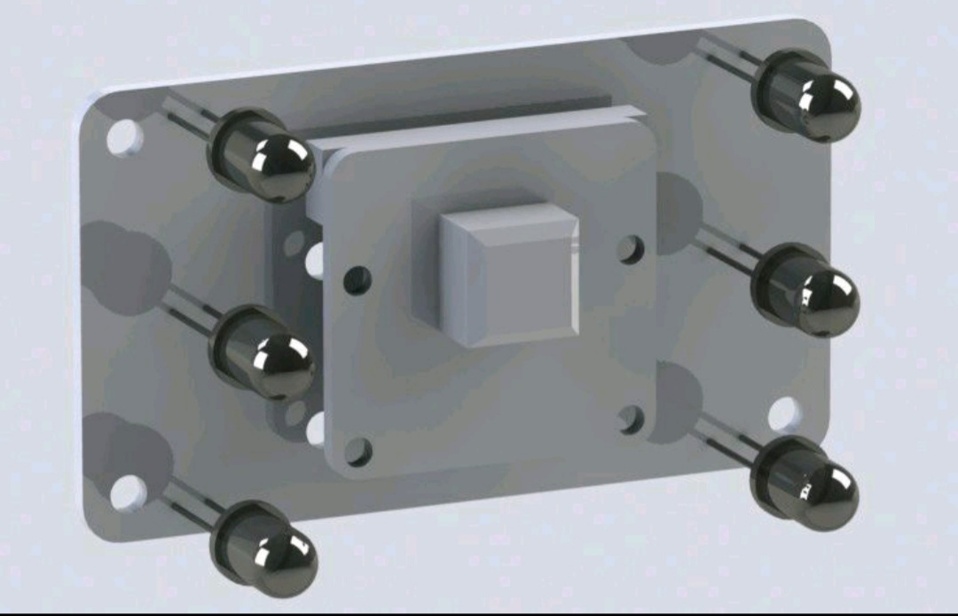
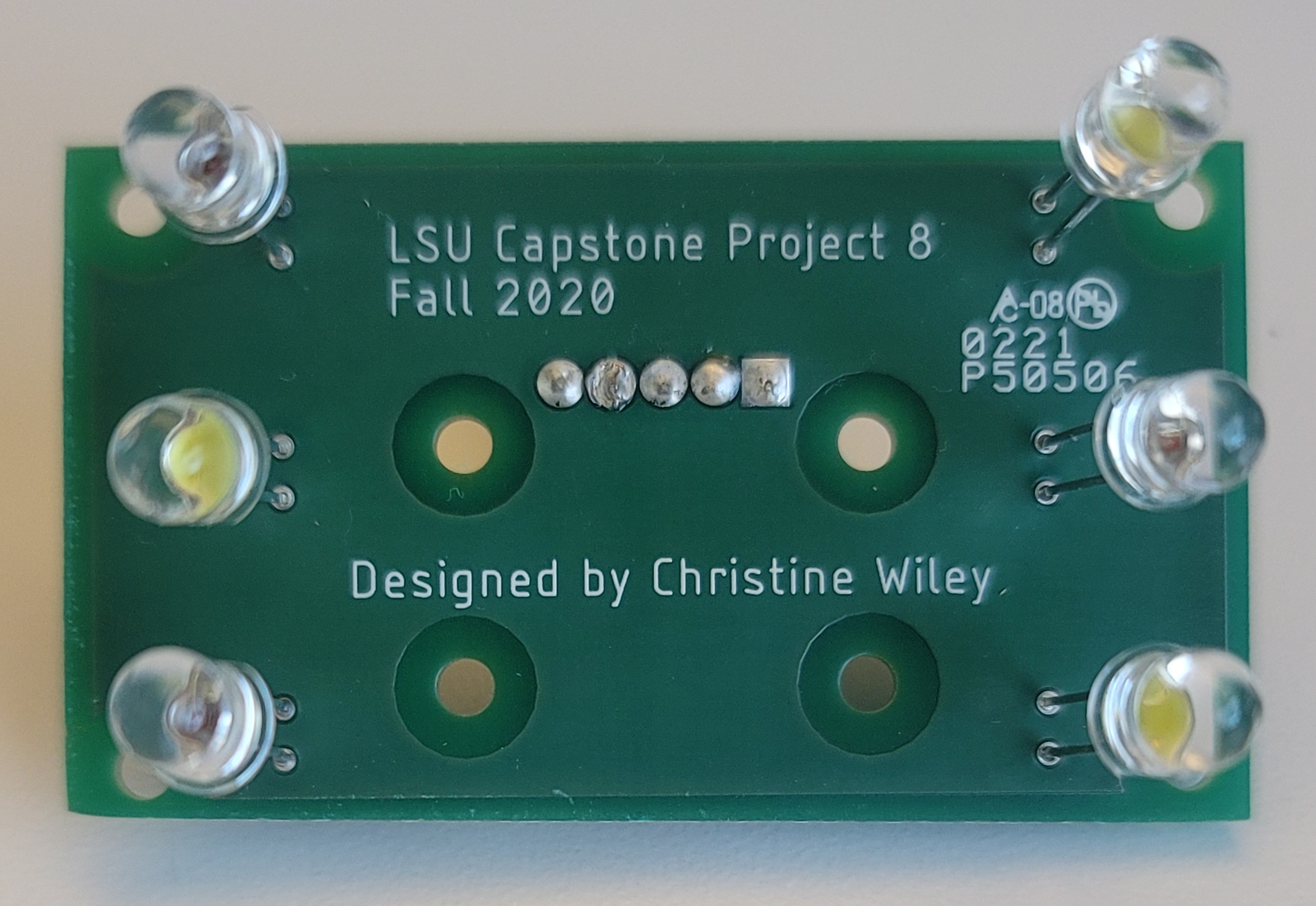
LED PCB Design and Assembly
Process design and assembly images for the lighting system
Designed and assembled by Christine B. Wiley
The following gallery illustrates the design process, for the lighting system on this handheld medical device. All images and diagrams below were produced by me except for the image illustrating the board dimensions and the CAD images with the camera module mounted in front of the board. Using the images provided by the mechanical engineer on our team, Gabriel Ragusa, I was able to construct a board that would adhere to design specifications required to meet a compact and handheld design requested by our sponsor. The first image is my schematic diagram for the lighting system created utilizing Eagle. Below it, my board file illustrates the arrangement of two types of LEDs which will be used to illuminate the skin of patients when operating the device. Finally, the boards were ordered and received from the manufacturer. This allowed me to perform validation and testing on the boards before hand soldering the individual components. Further testing is required to determine if this circuit will operate correctly when attached to the microcontroller.


The final design proposal for this project required discussion regarding types of analysis I intend to perform during Spring 2021 to validate the LED PCB. Below is my written and graded response to the prompt.
“Pullup Resistors: A strong pullup prevents the I2C pin from being able to drive low. The low level output voltage is read as a valid logical low by the IC’s input buffers and determines the minimum pullup resistance. During typical operation of the SDA pin, the maximum low output voltage is 0.6V and the low output current is 6mA, resulting in a minimum pullup resistance of 450 ohms for the I2C connections. For the enable pin, the maximum input clamp current recommended is +/-20mA also resulting in 450 ohms for the pullup resistor value.
White LED optical analysis: From the datasheet information, the white LEDs have a 25 degree angle of radiation and a typical luminous intensity of 18000mcd. At a working distance of 80mm, the approximate diameter of the light spot is 35.5mm. The triangle arrangement of the like LEDs shows the diameters of the light spots will not overlap. During testing, if there is significant shadow in the center of the light distribution affecting the percentage of accuracy of the diagnosis, it will be addressed with larger LEDs.
Amber LED optical analysis: From the datasheet information, the amber LEDs have a 30 degree angle of radiation and a typical luminous intensity of 6800mcd. At a working distance of 80mm, the approximate diameter of the light spot is 42.9mm. The triangle arrangement shows the diameters of the light spots will overlap and avoid creating shadows. Color rendering index (CRI) is a measurement of how a light source shows the “true” color of illuminated objects. CRI is an average of the first eight R values. R9 value is not included in this average and is the score of how accurately the color red is produced by a light source. Red is a critical color in applications reflecting accurate human skin tones. Light that lacks red will result in illuminated skin that is pale or green in appearance. For these reasons, amber LEDs are included in the design and a table illustrating the calculation of the CRI from the spectral power distribution (SPD) is located in the appendix.”

” This figure compares two graphs calculating CRI from SPD. The comparison uses wavelength and irradiance values from the amber LED datasheet in the bottom graph and compares it to calculated general and extended CRI values for a complete spectral distribution. This illustrates the R9 value provided by the amber LEDs.”
